Wafer inspection in the semiconductor industry is a complicated, multistage process. In this two part series, our experts at Motic will outline the basics of the inspection process, and how light microscopes can help during optical analysis.
Fundamentally, wafer inspection is split into two categories: unpatterned and patterned wafers. Generally, unpatterned inspection looks at defects on bare wafers. Patterned inspection looks at defects on processed wafers now containing circuitry.
Today we’ll be looking at unpatterned wafer inspection and how material microscopes should be used in this process.
Unpatterned or bare wafers come in many types of material depending on the application needs. Each wafer has their own specific characteristics. The most common wafer materials are Silicon, Gallium Arsenide, Germanium and Silicon Carbide (SiC). For example, SiC is widely used in power semiconductors and often focused in application areas such as the automotive industry.
Each of these unpatterned wafer types have inspection needs since defects can come about even in this early stage in the Semiconductor fabrication process. Reflected Light Microscopy contrasting techniques can be valuable aids in locating and identify many of the common defects. However unpatterned (bare) wafers can pose difficulty for light microscopy to find focus since by design they are highly polished clean surfaces with no features to focus on.
There is a simple way to use an aid to find focus. This can be accomplished in brightfield and DIC by slightly closing the field diaphragm so that it is visible in the field of view.
The field diaphragm is located in a conjugate image plane to the focal point of the objective lens. By focusing the image of the field diaphragm, you find the surface of the wafer.
Below are some examples of inspection and defects seen in bare wafers:
• Scratches which may have taken place during the polishing process (e.g., CMP) or handling.
• Scratches may be very fine in both lateral and depth dimensions and often not observed well in Brightfield contrast.
• Darkfield contrast provides an advantage since it utilizes scattered light from edges to provide a bright scratch on a black background, but this method makes it very difficult to find focus as mentioned above.
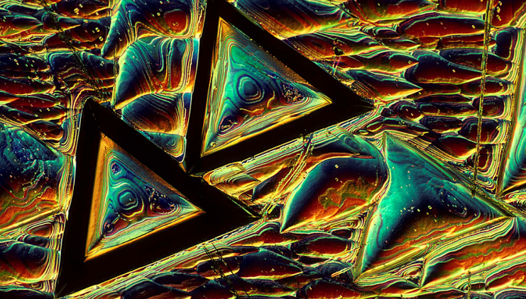
• The DIC contrast (differential interference contrast) technique can be useful since it can produce a change in contrast with change in depth and can be sensitive in the nanometer topographic range.
• DIC is a single shear directional technique and has maximum contrast with scratch perpendicular to its direction while low contrast when scratch is parallel.

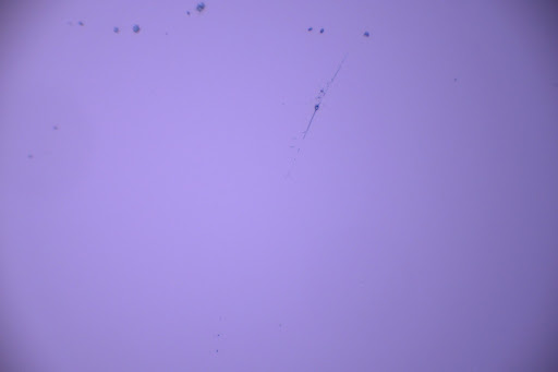
Scratches and contaminants, viewed under brightfield vs. darkfield
Stacking faults which are irregularities in the planar stacking of atoms in a crystallographic matrix which can affect the current flow in semiconductor devices.
DIC contrast (differential interference contrast) technique is highly sensitive to changes in local height topographies (in the nanometer range). With this technique stacking faults can be made visible.
The PA53MET holds all brightfield, darkfield and DIC options along with easy-to-use software for measurement and recordkeeping. The microscope also offers motorized xyz for more advanced imaging applications.
Copyright: Motic Scientific